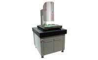
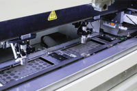
Sonoscan® has introduced the J610™, the latest member of its C-SAM® acoustic microscope line. The J610 is a semi-automated tool designed for production environments and has an unusually large scan area. Its key role is finding internal structural defects by screening trays of loose components, wafers, board-mounted components and other suitably sized items.
The 610mm x 610mm scan area can accommodate 6 JEDEC-style trays or one or more printed circuit boards. To reduce vibrations and maximize image quality, the system’s patented inertially balanced linear scanner is counterweighted.
The J610 can learn the x, y and z extent of specific user-defined areas of interest within a component.
By comparing anomalies to the user’s standards, it can automatically accept or reject components.
Using Sonoscan’s PolyGate™ software, it can create a separate image for each of multiple depths of interest in a given component, without increasing scan time.
Using Sonoscan’s proprietary Q-BAM™ module, it can create non-destructive cross sections through a component.
When scanning printed circuit boards, the system accurately finds and scans a component even if the component is slightly out of place on the board.
When defects repeatedly appear in the same component on multiple boards, steps can be taken to find and eliminate the cause.
J610 inspection permits replacement of board-mounted components that fail to meet the user’s criteria.
Sonoscan, Inc.
(847) 437-6400


