CMOS Sensors Continue to Advance
Consumer tech drives CMOS sensor advancements and lower costs, and delivers a boon for machine vision applications.

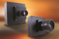
Cost and ease of integration will have a wide-reaching impact on the sensor market. Source: Teledyne DALSA
The cell phone industry has been the single largest driver of new CMOS image sensor technology for the past ten years—smaller pixels, higher sensitivity, and lower noise—all in a bid to decrease sensor cost and capture ever higher quality still and video imagery for human consumption. The size of the cell phone market has enabled the tremendous investment in the fabrication technologies required to achieve these advances. Smaller, adjacent markets like machine vision and medical imaging have taken advantage of this massive technology investment by re-using the same technologies. The recent proliferation of Global Shutter image sensors targeted to machine vision applications is a prime example of such technology leverage.
The mobile market continues to grow and will keep driving new technology development. However, the next phase of growth in imaging products will increasingly come from new high volume applications such as automotive, virtual/augmented reality, and life sciences. These new applications rely on non-traditional imaging modalities such as 3D vision, thermal infrared imaging, and sensitivity beyond the visible. The investment in these new imaging technologies will rival the investments made during the past 15 years for cell phone image capture. And once again, the machine vision industry will seek out opportunities to leverage these new technologies for industrial applications. By recognizing these new consumer applications and the technologies that they will drive, we can gather insights about what lies ahead in machine vision.
Image sensors in the driver’s seat
As more and more safety features are built into new vehicles, the automotive industry has become one of the fastest growing new applications for CMOS image sensors. Sensors have already appeared on cars, predominantly in rear-view visibility systems (i.e., backup cameras), and they are increasingly being used by advanced driver assistance systems (ADAS) for collision detection, blind spot monitoring and lane change assistance. Longer term, the development of self-driving or autonomous vehicles will also offer sensor manufacturers significant growth opportunities. It is predicted that within 10 years it will be common for vehicles to be equipped with 20 or more image sensors. The breadth of applications is large—forward-looking vision for detection of obstacles such as pedestrians or animals on the road, range finding for navigation, in-cockpit monitoring of an operator’s vital signs to ensure that they are not drowsy or distracted, etc. Infrared imaging and 3D vision are each receiving significant attention and investment in anticipation of demand from the automotive sector.
Which 3D technology will prevail?
Automotive applications require 3D capability for imaging on short (sub-meter), medium (a few meters), and long (up to few hundred meters) length scales. At least three competing optical technologies are competing for automotive applications: time-of-flight (ToF) is essentially radar with light, where a pulsed or time-modulated light source is used to calculate distance based on transit time and the speed of light; binocular vision enables 3D vision by having two sensors a set distance apart on the camera; and structured light projects a pattern onto a scene and then detects spatial shifts to interpret how far away an object is. No one technology is ideal for all length scales. Even within each of these technologies sub-classes exist that are better suited to one application than another—for example ToF technologies based on pulsed light vs. a modulated DC source. It is likely that some combination of all of these technologies will find use in automotive applications.
But automotive isn’t the only high volume market space looking for 3D capability— gesture control for gaming and for user interfaces (think interaction with a computer screen via hand gestures rather than a mouse) is also driving investment in 3D imaging technologies.
What opportunities will these 3D technologies enable in industrial applications? One application area that is ripe for 3D vision is robotics. All of the above mentioned technologies are already available commercially for robotic vision but they are expensive and often cumbersome—as high volume applications like automotive adopt these same technologies, their use in robotics will multiply as size, cost, and power all shrink. Industrial inspection and metrology is another class of industrial applications that anxiously awaits advances in 3D vision technology. Here the overlap in requirements with high volume applications is smaller—inspection and metrology typically require information on a sub-millimeter length scale (and in some cases down the sub-micron level). Structured light will likely be the preferred technology; however development is still required to push the boundaries of spatial accuracy and speed of acquisition.
See beyond the visible
Another area of technology development that is being driven by high volume applications is thermal infrared imaging. Thermal imaging allows us to see objects that are not visible to the human eye by detecting the heat emitted by these objects. Low resolution imagery from such devices is already available in some luxury car models to enable the detection of pedestrians and animals that are otherwise obscured by darkness or fog. As the cost of this technology shrinks, it will become ubiquitous in all automobiles. That cost shrink will likely be driven in part by cell phone applications; cell phone makers anticipate customer demand for thermal sensing on cell phones to detect security threats, for example, an individual lurking around a car in a dark parking lot.
Thermal imaging requires sensitivity to long-wave infrared (LWIR) light. Conventional silicon-based imaging technology is not capable of such detection. Microbolometer technology, in which heat is sensed via localized change in resistance, will be the technology of choice for high volume applications—it’s most important attribute is that it does not require cooling and therefore avoids the bulk and the cost associated with earlier thermal infrared technologies. Pixel sizes and shrinking and optical sensitivity is increasing, both of which are bringing thermal imaging closer to the tipping point where reduced cost will enable widespread adoption in high volume applications.
Recently, thermal imaging has started making significant inroads into many other industrial and commercial applications. Security and video surveillance use thermal imaging sensors to detect the movement of individuals, animals and objects at night. Thermal imaging is used in industrial settings to identify hot spots in equipment which may alert to incipient failures. Noncontact temperature monitoring or radiometrics is another technology that offers tremendous potential to drive microbolometer demand—as costs fall, radiometric imagery will become an important tool for industrial control of manufacturing processes.
Spectroscopy
Though somewhat further from widespread adoption, spectroscopic imaging is another candidate for high volume applications that will lead to new opportunities in machine vision. Spectroscopic image sensors gather information about the materials being imaged by detecting the spectral signatures associated with these materials—essentially the fingerprint of each material as captured by the peaks and valleys in a material’s absorption and reflection spectra. In addition to material identification, specific sub-sections of the optical spectrum can be isolated to highlight different materials that would otherwise be difficult to distinguish. The term for this type of imaging is referred to as hyperspectral imaging. One of the more commonly quoted uses in high volume applications is the detection of foreign or dangerous materials—for example, a hyperspectral imager mounted in a cell phone could alert diners to the presence of harmful bacteria or allergens. And such sensors mounted in rooms or automobiles could alert occupants to the presence of dangerous gases.
Spectroscopy is a centuries old technology; however, it requires bulky and expensive sensing equipment that have restricted its use to scientific applications. For this technology to be adopted more widely, spectrometers must be developed using smaller, less costly CMOS sensors. Several miniaturized technologies are being developed that are compatible with handheld applications; some of the most compact are based on filter technology that is applied directly to the surface of the image sensor.
Spectroscopy also benefits from the detection of light outside of the visible; the UV and IR parts of the spectrum are rich with information. Conventional CMOS image sensors are insensitive to UV light; however recent generations of cell phone imagers have adopted a technology called backside illumination (BSI) that provides response deep into the UV. Unlike front-side sensors, which have wiring and photon collection on the same surface, the circuitry on the BSI sensor is behind the light-receiving surface, which improves light collection efficiency. This is the motivation for use of this technology in conventional cell phone image sensors. Because they capture light directly on the silicon layer, BSI sensors offer more sensitivity across a broader spectrum—even in the ultraviolet.
It is easy to anticipate the broad use of spectral imaging technologies in machine vision as costs reduce. Spectral imaging will find greater use in industrial process control, for example, to aid in the detection of contaminants. Spectral imaging could also enable the detection of counterfeit products by purposely embedding markers with specific spectral signatures in product—otherwise invisible to the human eye, these markers would be instantly recognizable to a spectral imager.
Polarization: a technology in search of applications
Looking somewhat further down the road, polarization imaging is a new technology with promise for machine vision applications, though a high volume driver for this technology is more difficult to identify at present. Polarization is a fundamental property of light like intensity and wavelength. It not only identifies surface and geometry, but measures the physical properties of an object not seen by conventional imaging. Polarization can be used to detect when a material’s physical property changes due to defects. Stresses in transparent materials such as plastics and glasses, for example, are easily detected using polarization methods. Similarly, surface contaminants can be detected optically by detecting small differences in the polarization of reflected light.
An exciting future
The trends of the past 10 years are set to continue, and industrial imaging applications will reap the rewards. The demand for new imaging capabilities and technologies in high volume applications will provide excellent opportunities for re-use and extension into the industrial space.
Finally, it is important to note that two factors—cost and ease of integration—will have a wide-reaching impact on the CMOS sensor market. As the cost of image sensors decreases due to high volume, the number of applications using imaging will increase dramatically, leading to more silicon and higher sensor volume. Making sensors easier to integrate into cameras has the potential to drastically change the competitive landscape as it becomes more appealing for camera manufacturers to enter this fast-moving, high-growth industry.
Looking for a reprint of this article?
From high-res PDFs to custom plaques, order your copy today!


