For nearly 50 years CCD (charge-coupled device) sensors and CMOS (complementary metal-oxide semiconductor) sensors have competed on cost and performance in a wide range of digital imaging applications. Peltier coolers (thermoelectric modules) have cooled both technologies when the requirement demanded high-resolution images. Design engineers opted to use CCD’s for astrophotography, super-resolution microscopy, x-ray crystallography, and spectrophotometric assays. On the other hand, CMOS sensors made inexpensive digital photography a reality. Recently, CMOS sensors have made advances into areas traditionally held by CCD sensors, as well as emerging applications such as imaging for autonomous systems, machine vision & learning, and object detection & recognition. In these existing and new uses, active spot cooling using Peltier coolers (thermoelectric modules) have enabled these new and innovative CMOS sensors to outperform CCDs at a lower cost point.
Imaging Sensors
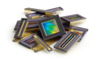
Digital cameras use two main types of imaging sensors: CCD (charge-coupled device) sensors and CMOS (complementary metal-oxide semiconductor) sensors. Both types of sensors perform the same function; converting light (photons) into an electrical charge (electrons) using an intricate 2-D array of photo-detectors (pixels). These individual buckets of charge are then amplified and digitized to create the digital image. The difference between the two main types of sensors is how and where this is accomplished.
In CCD sensors, the accumulated charge at each pixel is clocked row by row across the chip and then each row is read out cell by cell, where an off-chip low noise amplifier converts the charge to a voltage and then finally digitized by an analog-to-digital converter (ADC). Further digital processing reduces the average noise level and renders the final image. This tends to limit the read-out speed of the CCD sensor. Because CCD sensors are highly sensitive to temperature, multistage Peltier coolers (thermoelectric modules) are used to reduce temperature and limit dark noise current (thermally generated electrons produced in the absence of light). Since the low noise amplifier is off-chip, CCDs produce signals with minimal distortion, low noise, high resolution and excellent light sensitivity. Multistage Peltier coolers are able to reduce sensor temperature to -50⁰C with a 3 stage or -90ºC with a 4 stage allowing for long exposures used in astrophotography.
In CMOS sensors, each cell includes its own amplifier, and each column in the array typically has its own analog-to-digital converter (ADC), all on the same chip. This integration, distributed amplification and parallel output increases the CMOS sensor’s data transmission rate. Common fabrication of circuitry and photo-detector means CMOS sensors require fewer manufacturing steps, resulting in lower cost. In addition to faster frame rates and lower cost, CMOS sensor fabrication permits image processing functions directly on the chip. Noise reduction, auto-focus, auto exposure control, anti-jitter, motion tracking, color encoding and image compression functions all have been integrated directly on the chip.
CMOS Sensors
Continued advances in CMOS sensor technology have resulted in improved performance of these sensors across the electromagnetic spectrum, capturing high-resolution images in light spectrums not visible to the human eye. New CMOS sensor topologies have improved the quantum efficiency (QE) or the ability of the sensor to convert photons of light to electrons to be counted. These advances in CMOS technology and on-chip functionality have made it possible for them to be used in high-end scientific cameras. CMOS sensors are less sensitive to temperature than CCDs, but image quality can deteriorate as temperatures exceed 50ºC. Peak image resolution can be maintained at elevated temperatures by using Peltier coolers to keep temperatures below its maximum operating condition. This not only reduces dark noise on an absolute basis, but also maintains consistency between frames or operating modes for more effective noise cancellation. Reducing temperature results in lower dark noise enabling both the higher resolution and increased sensitivity at the high frame rates needed in machine learning applications. This breakthrough technology has increased the contrast and precision of digital imagery for the next generation digital inspection systems for examination of conditions such as residual stress, birefringence and surface roughness.
Emerging Applications
According to a recent study from IC Insights, CMOS image sensors continue to grab market share from CCDs. CMOS sensors have increased their market share to 89% in 2017, up from 74% in 2012. The market research firm also projects that 45% of CMOS image sensor consumption will come from applications other than camera phones. This includes next-generation camera designs for promising new applications like augmented and virtual reality. Object detection and recognition systems in advanced autonomous vehicle and driver assistance systems (ADAS) rely heavily on CMOS image sensors.
CMOS image sensor designs provide precise digital imaging solutions in consumer, industrial and machine-vision applications. Significant progress in CMOS image sensor technology includes more advanced pixel architectures, while many of these devices are integrating more functions to facilitate artificial intelligence and machine learning applications such as facial recognition.
Machine vision for robots, drones, optical character recognition, barcode readers, scanners, astronomical and satellite photography and the enhancement of radar images for weather forecasting are other examples of CMOS imaging sensor use cases. CMOS sensor technology impacts areas beyond imaging, such as humidity and temperature sensors, X-ray detectors, micro-hotplates and sensors for fluid flow.
Thermal Challenges
Thermal noise causes CMOS sensors to lose image resolution as temperature increases. A rough approximation shows that dark current doubles for every 6°C rise in temperature. A 20°C drop in temperature could reduce the noise floor by 10dB, thereby improving dynamic range by 10 dB. In outdoor environments temperatures can exceed 40°C. To prevent image quality from deteriorating, high temperature Peltier coolers can be used to reduce the sensor’s temperature below its maximum operating temperature and maintain high image resolution.
Spot cooling of the CMOS sensors in high-end machine vision applications can present significant challenges. The addition of Peltier cooling devices will increase the size, cost, weight and complexity of the imaging system. Cooling the imaging sensors can result in condensation due to surfaces exposed to temperatures below dew point. Many systems are in a vacuum environment with insulated surfaces on the exterior to prevent condensation build up over time.
Heat rejection with passive cooling can be quite low. Limitations to proper airflow can result in an inefficient design that cools several degrees above ambient. This temperature may be above the CMOS sensor’s maximum operating temperature limit. This can occur quite often in outdoor applications and may require active cooling. Peltier cooling also adds heat to the heat rejection path requiring a heat exchanger with more capacity to dissipate heat into the air environment. Fan cooling or in some cases liquid cooling is required to sufficiently dissipate heat and keep thermal resistance of hot side heat exchanger down.
In addition to thermal requirements, assembly considerations play a role when optimizing for an efficient cooling solution. For example, outgassing is not acceptable because it can coat the imaging sensor optics. It is therefore vital to properly select thermal interface materials between the Peltier cooler and CMOS sensor with low outgas characteristics or substitute interface material, all together with a pre-tin solder on hot and cold surfaces of the Peltier cooler. Design considerations need to be made to minimize thermal shorting. This occurs when cold side surfaces come in contact with hot side surfaces which causes the Peltier cooler to draw more current to achieve the same cooling performance.
Thermal Solutions
The image quality of a CMOS sensor degrades at temperatures typically in the 50 to 60ºC range based on the quality of the sensor. For indoor applications, a free convection heat sink with interface material may be sufficient to cool a CMOS sensor with adequate airflow to just above ambient. It’s important to design a heat sink with maximum surface-to-air contact to reduce the overall thermal resistance. Typically, space constraints make it difficult to accommodate a properly sized heat sink and forced air is required to keep the temperature just a few degrees above ambient.
For most outdoor applications these thermal solutions will not be enough. Heat from surrounding electronic components can exceed the upper temperature limit of the CMOS sensor and require a Peltier cooling solution. The thermoelectric module creates a temperature differential across it, lowering the temperature of the critical CMOS sensor by as much as 40°C from the hot side temperature of the heat sink. If the hot side heat sink is at 90ºC, a Peltier can cool the CMOS sensor down to a temperature of 40ºC if required.
Conclusion
The trend to combine high-end imaging systems for outdoor environments drives the evolution of active cooling solutions – particularly in applications using CMOS imaging sensors. High-end machine vision imaging systems require active cooling to ensure optimal image resolution. Otherwise, high temperatures can cause degradation in ability to interpret image. Designing thermoelectric modules into the imaging systems keeps the CMOS sensor from approaching its maximum operating temperature limit which results in higher resolution image quality.
For more information, visit www.lairdthermal.com/.


