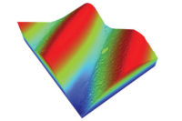
Bruker Secures Orders for SP9900+ 3-D Optical Mi-croscope
BILLERICA, MA—Bruker has received more than $7 million in orders for its new Bruker SP9900+ high-throughput high density interconnect (HDI) substrate metrology system, and has begun shipping the product in volume. The SP9900+ Large Format 3D Optical Microscope is specially designed for the semiconductor packaging industry.
"Manufacturers of multichip modules (MCM) and high pin count semiconductor chips are continually increasing panel sizes, reducing feature sizes and increasing the pin count of their products, which creates new challenges in process control for high-volume production," says Mark R. Munch, president, Bruker MAT Group and Bruker Nano Surfaces Division. "The most important areas typically involve measurement of traces, vias, and interconnects, as well as the surface roughness of copper and Ajinomoto build-up film. Working closely with our customers, we've been able to reduce the 'time to measurement' for these critical inspection challenges to less than one half of previous generation systems."
Looking for a reprint of this article?
From high-res PDFs to custom plaques, order your copy today!


